











Thin Layers
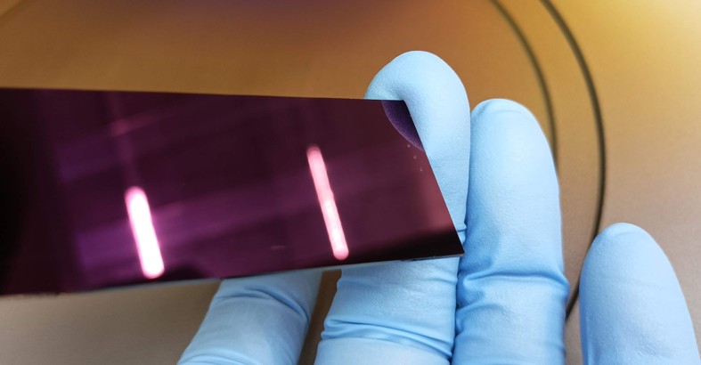
The Thin Films Group builds on decades of experience in plasma-assisted deposition of thin coatings and in the mechanical characterisation of materials. The group began to take shape in the 1980 s in response to the growing demand for surface engineering and functional thin coatings for cold cathodes of gas lasers and wear-resistant components used in lithographic systems. To support the characterisation and development of these advanced coating systems, a unique dynamic impact testing methodology has been developed at the Institute since the second half of the 1990 s.
With the introduction of additional deposition technologies, the portfolio of deposited coatings gradually expanded from nanometre-scale coatings with precisely controlled properties for X-ray optics to micrometre-thick wear-resistant protective coatings for engineering applications.
Today, our facility is equipped with two magnetron sputtering systems and one auxiliary thermal evaporation unit. We maintain an inventory of over thirty metallic and ceramic targets. By integrating reactive gases, e.g. nitrogen or oxygen, into the sputtering process, we can further expand our vast range of deposited materials. Currently, our R&D is primarily focused on thin film applications for optics, electronics, electron microscopy, and semiconductor technologies.
Our comprehensive thin film characterization capabilities are highlighted by our continuously advancing dynamic impact testing method. This technique, which relies on repeatedly striking a sample surface under strictly controlled parameters, has expanded far beyond thin PVD coatings. We now routinely test a wide variety of materials, including untreated bulk samples and modern materials produced via additive manufacturing (such as 3D-printed metals and cold-sprayed components).
We actively apply our expertise through scientific grant projects and research partnerships with both academic institutions and industrial partners.
