


Electron microscopy under ultrahigh vacuum conditions
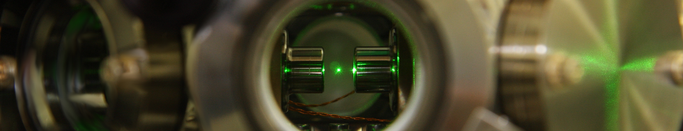
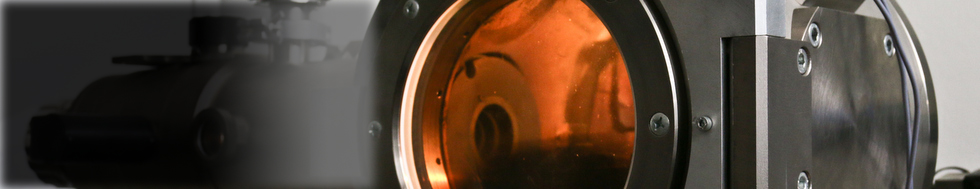
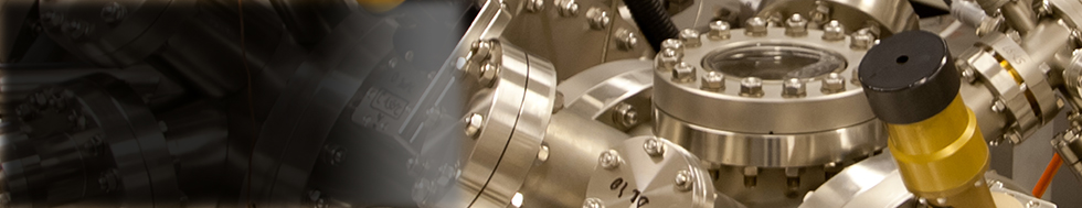
Microscopy and the analysis of very clean surfaces under ultrahigh vacuum conditions represent an irreplaceable tool for contemporary and, in particular, new nanotechnologies. ISI has built its own version of the ultrahigh vacuum scanning electron microscope for examination of atomically clean and defined or even in-situ prepared surfaces of solids. The microscope has an operational vacuum of 10–8 Pa thanks to its complete bakeability, but samples are readily exchanged via vacuum airlock. The device is composed of three vacuum chambers: the observation chamber, preparation chamber and airlock. In the observation chamber the electron optical column enables one to work at all electron energies down to fractions of eV or even to acquire the mirror image of the sample. Detectors available include acquisition of the complete backscattered emission at all energies, secondary electron emission, transmitted electron emission and detection and analysis of gases released by electrons. The device will soon be equipped with an energy analyzer of Auger electrons. In the preparation chamber devices are available for ion beam cleaning and sputtering of the sample surface and for evaporation of up to three different materials.
ISI plans to purchase a photoemission electron microscope combined with a direct imaging low energy electron microscope for complex examination of clean crystalline surfaces of all kinds.
Advantages and application examples:
- The unique sample stage/detector assembly enables the adjustment of the device for perfect performance at arbitrarily low energies.
- The electric field above the sample collects the complete emission and hence provides full available information.
- A very high collection efficiency of signal detection increases the signal-to-noise ratio in images and speeds up data acquisition.
- At very low energies novel contrast mechanisms appear in micrographs, revealing the electronic and crystalline structure in addition to the conventional topographic and material contrast.
- Small interaction volume substantially improves the resolution of details immersed below or protruding above the surface and the surface sensitivity in general.
- Grains in polycrystals become visible in high contrast, including subgrains, twins, etc., with the possibility of identifying their orientation.
- Internal stress in polycrystalline materials is mapped in high contrast and resolution.
- The doped areas in semiconductors can be quantitatively examined and critical dimensions measured exactly.
- At very low energies the radiation damage of extremely sensitive samples ceases.
- Thanks to their longer wavelength very slow electrons produce diffraction and interference phenomena, providing novel tools for the examination of nanostructures.